Class E Power Amplifier Design
Alan Melia G3NYK, Mike Probert GW4HXO, and Finbar O'Connor EI0CF
There have been many different configurations that have attempted to squeeze the best efficiency out of an RF Power Amplifier. Class E is a form of 'switching' amplifier which was patened by Nathan Sokal WA1HQC in around 1976. I first saw it described in Design Electronics in 1977. Being an amateur, Nat is an extremely practical man and the article gave a test circuit that could easily be assembled from laboratory components, and then measured whilst the components were altered. I had little interest at that time but the article was filed away until I had attempted to modify an audio amp for 73kHz with very little success. I dug out the old article and read it several times. It did not give any guidance about where to start from in a new design, though it gave a number of optimised equations for calculating the critical component values. I started by putting the equations into a spreadsheet and tried some numbers to see what changed, with power, supply voltage and load. As a result I think I gained a feeling for the circuit and developed a 'recipe' for the process of proceeding through a design
The following notes are a result of experimental work, and in no way add to the theory which has been adequately covered by Nat and Fred Raab in many papers.
My objective was to try and formulate an easy route to a medium power 136kHz power amplifier, which would be relatively benign. By benign I mean a circuit that did not have an insatiable appetite for FETs. The RSGB LF reflector has carried stories from time to time of exploding FETs and of complex protection circuits to circumvent this problem. My naive thinking was that a switch which is either on or off should form the basis for the circuit, using a single ended design to avoid the "cross-coupled oscillator effect". It seemed that some LFers had already been playing on the verge of Class-E but there was no information with the circuits and it seemed they did not really know how it worked or how to set it up. Unlike many PAs that we are familiar with, you cannot just increase or decrease the power from a Class E PA by varying the loading on it. The first important thing to appreciate is that a Class E PA is designed for a particular power output, and it will only be efficient at this 'design' power level.
Click here to download Excel worksheet
Design proceedure
1. Select a Power Supply voltage (Vdd).
2. This determines the Vdd(max) of the FET at approximately 3.5
times Vdd
3. Select the target power level
-------- This determines the optimum value of C1 and the optimum
load impedance
4. Determine the the value of C2 and L2 from the Excel worksheet
Nat's original paper didn't give guidance but his later QEX paper suggests that the value of the choke L1 is not critical, but it should have an inductance with a reactance at least 30 times the optimum load impedance. this means at 136kHz a minimum of around 500uH. I have been using a choke of 5mH as I want to operate at 73kHz as well. Also I suspect that the larger choke will give a 'softer' keying risetime.
Now for some practical details. The point of Class E is that there is no power wasted other than the Idss*rds(on). This is achieve by the series circuit C2L2. Because C2 will have to be made up from standard values of pulse rated HV capacitors it is necessary to have some adjustment on L2 for initial set up. You will see in the worksheet a column which calculates the resonant frequency of L2C2, and may be somewhat surprised to see that it differs from the driving frequency. This is because this circuit is NOT a tuned circuit to extract the power at 136kHz. It is part of a 'flywheel' circuit to ensure that the correct voltage waveform can be generated at the FET drain, during the FET 'off' period. The drive waveform for maximum efficiency should be a 50:50 squarewave of about 10volts amplitude (see the drive circuits on Dave G3YXM's PA and Dave G0MRFs design). Dropping close to ground on the off periods. The circuit is matched to 50 ohms by a ferrite transformer. the rule-of-thumb for ferrite transformers is to make the (unloaded) reactance of the winding at least three times the impedance it is fed from. Thus if the optimum load impedance 'R' is given as 10 ohms by the worksheet, the inductance of the primary should be 10*3/2*pi*f. Because we are only interested in a narrow range of frequencies, I have used 5 times rather than 3 times. This makes the secondary taps a little finer, and makes it easier to find the maximum power position.
The vital part of the set-up proceedure is to monitor the drain waveform on an oscilloscope. As the FET switches off the current is maintaned by the choke and starts to flow into the capacitor C1. As the capacitor C1 charges up current starts to flow through the load via the series circuit C2L2. After the voltage across C1 reaches about 3 times the supply voltage the load draws curren from C1 and the voltage starts to fall. To achieve the maximum efficiency the voltage across C1 should fall to zero by the time the FET is switched on again. This ensures that the FET does not wastefully discharge C1.Any discharge by the FET at this point of the cycle does not generate any RF power in the load. It is even more complex than that for the slope of the voltage waveform should also flatten to reach zero volts, with a kind of 'soft landing'. This is the condition that will yield maximum efficiency. This waveform and how it depends on C1 and C2 and L2 is described in the QEX article Jan.Feb 2001 pg 9. "Class-E RF Power Amplifiers" by Nathan Sokal.
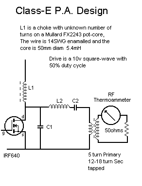
I have achieved 175 watts for a DC input of 190 watts (38 volts at 5 amps) using a single IRF640 which is a cheap TO220 packaged device. The drive was not keyed for long but the FET did not seem to show any signs of distress, despite a very small heat sink. The IRF640 is a 200volt device so the absolute supply limit is about 55volts. Mike GW4HXO has also achieved similar levels and is constructing a dual (parallel) FET 300 watt version on a sizable heat sink. Finbar EI0CF has used a different configuration but has achieved powers of about 530 watts, at efficiencies that we think, allowing for RF ammeter inacuracies must be over 90%. Finbar uses two 500volt IRFP devices (better heat sinking...more expensive) and a supply voltage of up to 90 volts. He also used the scope trace of the FET drain waveform to optimise the set-up, despite a totally different reactive network. Mike's and my experiments have been carried out into dummy loads only but Finbar has fired the 500 watts into an aerial (I dont think he has a dummy load that big .....yet.)
The one pleasing thing is that none of us has lost a single FET in these experiments. The worst condition is probably a short circuit load, any other condition seems to reduce the power drawn by the FET. Even a very low load impedance seems to damp the circuit somewhat. It may seem daunting to have a scope attached to the TX all the time. This is really only necessary in the early stages of set up. Once the circuit is set with the correct component values. the PA can just be switched on and keyed. If it is necessary to tune the aerial. The supply voltage can be reduced, this does give sub-optimum efficiency but does provide reduced dissipation as well. The PA components C1 C2 and L2, and the transformer tap should NOT be altered but the loading coil should be tuned for maximum aerial current.** addition 7/2/02** Johan SM6LKM has suggested that it is not quite right to tune for maximum current as the maximum output power of a Class-E stage does not coincide with the condition of maximum efficiency. The alternative would be to use a bridge such as that described by Jim M0BMU in the LF Experimenters Handbook to adjust the aerial to a true resistive match. Another aternative is to use the simple transformer bridge to adjust the aerial tuning first see my aerial measurements page **
If aerial matching is employed this should be adjusted to present the transformer secondary with 50 ohms. The supply may then be switched up to full voltage and the PA keyed. If Q values of around 10 are used for the 'flywheel' circuit (see the worksheet) the PA will not need any adustment across the whole of the 136khz band. It may be possible to switch C1 and C2 and use the same coil L2 (differnet tap) to use the PA on 73 kHz as well (at least that is what I am hoping)
There is a lot written about Class-E and its variants. It is used right up into the microwave bands for FM and digital TX stages. I have just 6 papers, and they are covered in mathematical 'squiggles'. Fortunately we don't need to be able to understand the Maths to use the idea !!
I have also recently used a simulation program called SIMetrix (a free download from NewberryTech) to plot waveforms for different circuit values, and have found this very instructive.
For another design program check Jim Tonne's web site at http://www.qsl.net/wb6bld/software.html (Dead)
TAILPIECE
One would expect a square wave drive PA to be horribly dirty with harmonics, the Class-E stage is NOT. If we use a design Q of 8 to 10 the output waveform only has about 1% harmonic distortion, when set up properly. I think this is due to the optimum adjustment of the flywheel circuit. I believe with a high Q LF aerial, this almost makes further filters unnecessary. I need to do more work with the analyser before I will stand by that assertion, though.
The graphs below were produced from the simulator SIMetrix. The first shows the drain voltage and drain current with too little inductance in L2. Note the big spike of current as the FET discarges C! which has not reached zero volts at FET switch-on
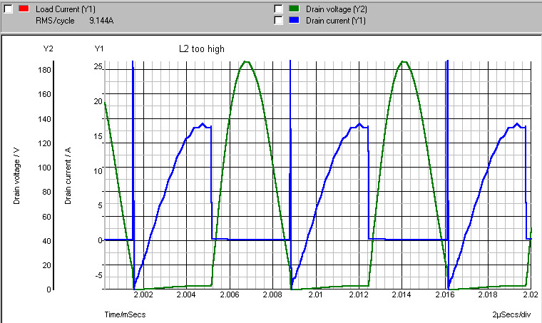
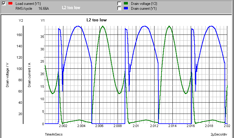
The second graph shows the results of too little inductance in L2. The load current is higher but there is a wide high wasteful spike of current through the FET at switch-on. This current spike is just heating the FET. Notice also the voltage waveform did not reach zero and is rising again by the time the FET switches on. There is about 80 volts across C1 which the FET discharges.
The final graph show the situation at near optimum. There is still a little spike at swtch-on, but the voltage waveform is down to zero and is almost flattened out. Although Nat suggests monitoring FET current in his 1977 article, it would seem to be only necessary to monitor the drain voltage. The adjustment is quite critical, but you know when it is right.
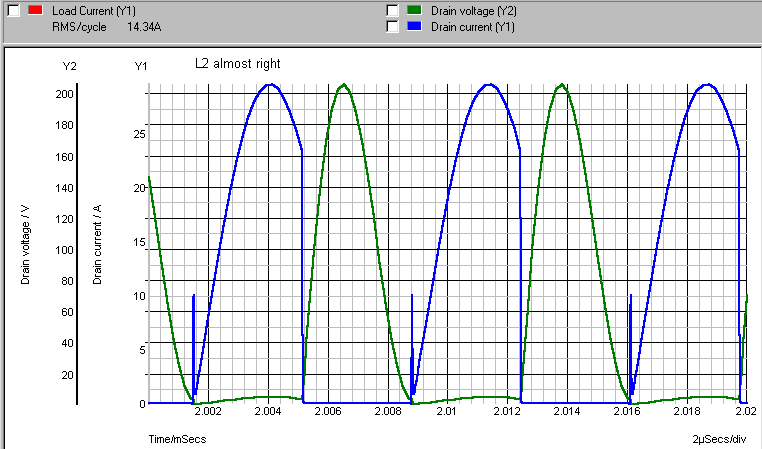
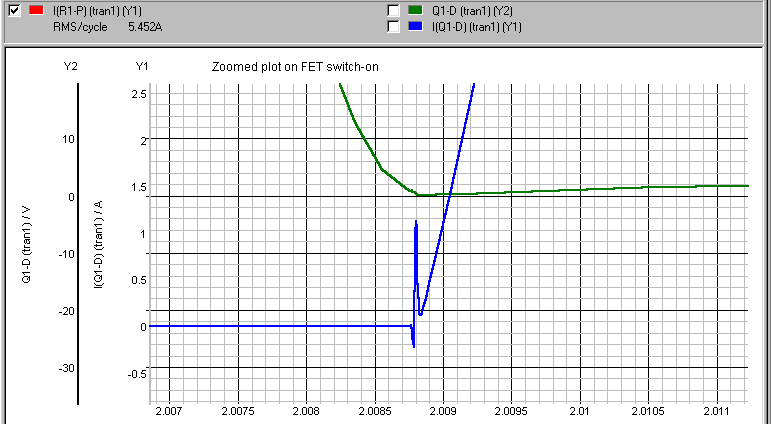
The plot below is a zoomed version of the waveform at the drain (green) showing that the profile is flattening out, but the gradient (slope) of the waveform is not zero when the fet switches on. That is the reason for the small current transient *blue) and some of the loss. This plot was produced later than the above and may not be for exactly the same component values, hence different current and voltage scales.