A 500kHz Transmitter design
by Jim Moritz M0BMU
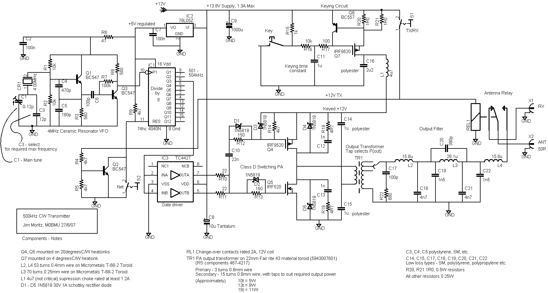
I drew up a circuit diagram of my new 500kHz transmitter design in case anyone is interested.
It uses a "half-bridge" voltage-switching class D PA with complementary N and P channel mosfets. The idea of this is that the push-pull design minimises 2nd harmonic levels at around 1MHz, and the complementary mosfets simplify the gate drive requirements somewhat. It uses cheap IRF520 and IRF9520 devices, and produces a maximum output of about 11W with 13.8V DC supply. It can easily run at different power levels by changing the numberof turns on the output transformer. I included DC current limiting in the keying circuit, which allows the PA to operate into open, short, and reactive loads without apparent distress. It has a VFO based on a 4MHz ceramic resonator and divide-by-8 counter. This covered the whole band with several resonators I tried, and drifts by a few hertz per hour, which is satisfactory for most purposes.
The circuit diagram (click here) is the basic CW transmitter for now. I have also added various other bits and pieces such as variable output power, FSK for DFCW, and a RF voltage/current/phase output metering system for easy antenna tuning, but will have to draw these up later.
Cheers, Jim Moritz